Alder Lake-S Review
Update: 11-26-2021 - L3 Latency * P-Core BW Results Updated
Introduction
After running Intel’s X58 & 1st Generation CPU for over a decade I have finally decided to upgrade to Intel’s latest and greatest, the 12th Generation Alder Lake-S CPU. There had been plenty of leaks and information leading up to Alder Lake formal reveal, but nothing was official. Intel’s Alder Lake was officially launched on October 27th 2021 and Intel also allowed pre-orders to begin. Alder Lake was officially released on November 4th 2021. Now with official information coming from Intel including the price, specifications, overclocking information and performance numbers; there was plenty to look forward to. Intel revealed that six Alder Lake CPUs would be released on their 10nm cores along with DDR5. In addition to those 6 CPUs for the consumer desktop segment there will be approximately 60 CPUs released across the entire Alder Lake CPU stack for different industries. More than 10 years ago I felt as if I had the cutting edge in technology. My Intel X58 platform included tech such as USB 3.0, SATA 3 & SATA6 ports, dual PCIe 2.0 (x16) slots, one PCIe 2.0 (x4), hardware & software RAID 0, 1, 5 &10, Triple Channel DDR3 1866Mhz+, eSATA 3.0, x2 FireWire and all other types of cool tech during that era. Throughout this article you will notice that I will make comparisons to my Intel 1st Generation CPU as a reference. Looking at the 12th Generation “Alder Lake” CPU and the Z690 chipset more than a decade later we see DDR4-3200Mhz & DDR5-4800Mhz supported, PCIe 5.0 (x16) & PCIe 4.0 (x4) connected directly to the CPU. My 1st Gen microarchitecture only supported DRAM (DDR3) connected directly to the CPU. Other nice 12th Gen technology includes M.2 slots, USB 3, but not the same USB 3 that my X58 motherboard used, Intel’s Z690 boards supports USB3 5G, 10G and 20G. So for me personally this should be a massive upgrade since I have skipped so many releases from both Intel and AMD. Intel’s Alder Lake-S has grabbed my attention and I am excited about the new microarchitecture. Unlike previous microarchitectures from Intel, Alder Lake is taking a page from ARM’s “big.LITTLE” configuration setup. Alder Lake contains larger P (Performance) Cores and smaller E (Efficient) Cores. Windows 11 will be required to take full advantage of Alder Lake’s P-Cores and E-Cores, but I will speak more on that later. It’s amazing to learn and see how Intel’s microarchitecture will perform with a hybrid design. For those who haven’t been following Intel and all of the news over the past several years I’ll try my best to get you up to speed quickly.
Alder Lake-S YouTube Video
Intel 10nm & Delays
For roughly a decade Intel’s proven “Tick-Tock” model worked well which allowed Intel to create a new microarchitecture on existing fabrications before ramping up a smaller node. All good things must come to an end right? Well it did come to an end and in early 2016 Intel replaced the “Tick-Tock” model and revealed a new model called the “Process-Architecture-Optimization”. In 2016 Intel was officially one year behind with their 10nm release and was still using the 14nm architecture, which was also delayed by roughly a year in late 2014. So from 2014 to 2021 consumers have seen Intel optimize their micro-architectures based on the 14nm fabrication (Skylake) using the “Process-Architecture-Optimization” model. Most recently in 2021 Intel has revived their “Tick-Tock” strategy; however it is safe to say that Intel will be continuing their “Process-Architecture-Optimization” model as well. Intel’s 10nm ramping didn’t go as planned in 2016 due to yield defects and other fabrication issues surrounding the 10nm node until around Q3 2018. In 2018 Intel finally released their first 10nm CPU (Cannon Lake), but it was only a 2 Core \ 4 Thread mobile CPU with a TDP of 15Watts. The operating frequency was 2.20GHz and boosted to only 3.20GHz. That’s not much for being roughly 3 years late to the market.
AMD Is Rising & Intel Nodes Renamed
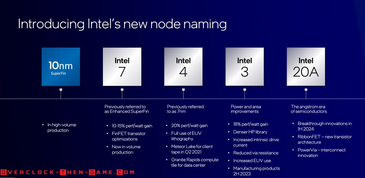
While Intel fell behind with their smaller node (10nm) fabrication this has given AMD plenty of time to catch up with the help of TSMC. AMD has been working on interesting technology over the years ranging from multi-chip modules to Infinity fabric and most recently V-Cache with their Ryzen, Threadripper and Epyc brands. AMD has also regained market share and has overtaken Intel in stock market price. Intel’s node naming scheme has been changed as well. Intel has noticed that consumers have taken precedence in the naming schemes for nodes (i.e 14nm vs 10nm vs 7nm vs 5nm), while leaving out other important details within microarchitecture & process specs for the fabrications. This is also due to the fact that other industry leaders such as Samsung & TSMC etc. have been using different metrics to name their fabrications while Intel has continued to follow the traditional metrics for naming their nodes. Consumers just believe smaller is better when there are many more things to consider in the equation.
Alder Lake Cove’s and Mont’s
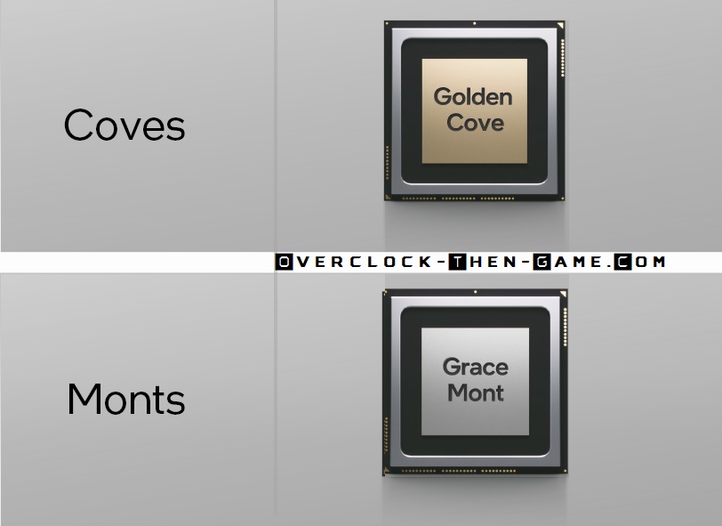
Prior to Alder Lake Intel released their first “Hybrid Technology” based on the “Lakefield” 10nm processor. Lakefield contained 10nm “Sunny Coves” for performance related workloads. In addition to the Lakefield Sunny Cove uarch Intel had “efficient” 10nm “Tremont Cores” as well. This was Intel’s first attempt using their “Hybrid Technology” rollout which was only available on the mobile platforms. Alder Lake is Intel’s very first Desktop CPU to use their Hybrid Technology. Intel's' Alder Lake microarchitecture contains Coves (Performance Cores) and Monts (Efficient Cores). I believe it is a safe bet to conclude that Monts means “Mountains” at this point. The Performance (P)-Cores in this case are the “Golden Cove” CPU uarch (CPU micro-architecture) and the Efficient (E)-Cores are the “Gracemont” uarch. The Golden Coves (Performance) Cores contain Hyper Threading capabilities and are the high performance work horses that we expect. However, on the other hand we have Gracemont (Efficient) Cores which lacks Hyper-Threading, but has been designed for throughput for light background tasks in many cases. This should allow the CPU to use as little power as possible when you aren’t taking full advantage of Alder Lake CPU performance. The 12th Generation Alder Lake processor uses Intel's LGA1700 socket which means that it has 500 more pins than the previous socket (LGA 1200 - 11th Gen Rocket Lake). Intel is known to ensure that their sockets stay roughly the same and that has been the case over the years, however a major redesign was in order for the Alder Lake CPU packaging and the LGA socket. This would make previously released CPU coolers obsolete in some cases for various reasons; however some manufactures will be offering upgradable brackets that will allow current LGA1200 CPU cooling solutions to be compatible with Alder Lake’s LGA 1700 socket. Some motherboard manufactures have both the LGA1200 and LGA1700 cutouts on the motherboard that will allow LGA1200 CPU coolers to be used with Alder Lake. There are a few concerns regarding the height and pressure and I will be taking a look at this later in the article.
- Prev
- Next >>